Who We are ?
-------A professional PCBA, Charging Locker manufacturer and
solution provider.
Betterliv Technology Co., Ltd is a professional manufacturer
and exporter of PCBA and Charging Locker. It is a
reliable and trusted supplier. As WPC member, most of products has
passed QI,CE,Rohs,FCC. With the concept “smart, health &
taste”, we built the product line for charging lockers and PCBA
products. We have a strong technical team, design team and
production capacity. We have an independent SMT production line and
reliability test equipment laboratory.
In pursuit of our vision to become a preferred choice of better
living experience, a new lifestyle to our customers, and our
mission to improve the quality of people’s lives, we leverage the
innovative talents to design and develop the innovative and
user-friendly products. And we differentiate ourselves from those
competitors on a basis of forward thinking, open and market-driven
mindset.
We embrace the values of of customer satisfaction, operational
excellence and innovation provide our customers with satisfying
deliverables.
What products we do?
------- Produce and customize various PCBA and Charging Locker.
Power PCBA
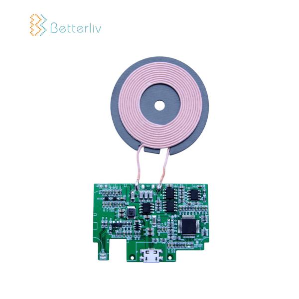
Wireless charger PCBA
Bluetooth Module PCB
Small OLED Display
Wireless Charger Receiver Module
2 Layer PCB Board
4 Layer PCB Board
6 Layer PCB Board
8 Layer PCB Board
Wireless Charger Coil
Mobile Phone Charging Lockers
Automatic Hand Sanitizer Dispenser Stand
Electromagnetic Solenoid Lock
Our Mission
------- Improve the quality of people's lives.
Our VisionOur Vision
------- To become a preferred choice of better living
experience.
Our Values
------- Excellence, innovation and respect constitutes our
culture for associates, business partners and customers. Each of us
is fully committed to serving our customers with good performance
and accomplishment what we do.


